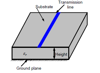
Simple T-line and its performance:
T-line
is just a line with a defined length and width on the upper surface of the
substrate which is created by removing copper coating from the surface except
the desired region. The figure is shown below where the blue region is a
typical T-line whose length is 100 mm and width is 2.2642 mm (calculated by
PCAAD for 50Ω microstrip T-line where dielectric constant of the substrate is
2.45 and thickness is 31 mils).
Fig. 5.1: Geometry of a standard 50-ohm microstrip transmission line on a substrate whose dielectric constant is 2.45 and thickness is 31 mils.
S-Parameter
Performance of a microstrip T-line:
S-Parameter
performances are inspected from the plotted curves of the simulation by Zeland
ie3d where the curves of S11 (return loss) and S21 (insertion loss) are only
shown here. Stopband and passband yield the frequency band width of insertion
loss and return loss at -20 dB and -10 dB respectively. The following graph is
plotted by Grapher software by taking simulated data from the Zeland ie3d
Fig. 5.2: S-parameter performance of
50 Ω T-line whose length is 100 mm and width is
2.2642 mm.
Within
the range of 0-20GHz the signal has transmitted between two ports with
negligible
loss
and there is no stopband formed. The return loss performance of the ideal
microstrip
line
over the whole frequency range is also excellent and < - 10 dB. Since, there
is no
appreciable
insertion loss observed at the s-parameter performance of the T-line, therefore
it
characterizes an ideal transmission line.
Design of uniform circular PBGSs for Harmonic Suppression
Uniform
circular PBGSs are implemented to form different designs. PBG assisted BPF with
different lattices and PBG elements have been investigated that include (i) BPF
on 2-D array of uniform circular PBGSs which forms square lattice, (ii) BPF on dense 2-D uniform circular PBGSs
that forms rectangular lattice, (iii) BPF on 1-D uniform circular PBGSs that
exactly located under the two extreme 50-ohm lines and the central coupled
line, (iv) BPF on uniform circular PBGSs that are located under two extreme
line only and finally (v) BPF on uniform circular PBGSs that are located under
all the lines of a BPF. All these designs are shown in Fig. 6.20. These
investigations are very useful to understand the behavior of poles of BPFs in
the presence of PBGSs.
· Standard BPF
A 4-section asymmetric coupled line BPF is shown in Fig.
6.20(a). The dimensions of the coupled lines are: W1 = 0.425 mm, W2 = 0.525 mm,
G1 = 0.2 mm, G2 = 0.7 mm, L1 = L2 = 3.625 mm and W50 = 0.6 mm. The dimensions
of the reference BPF are same as [32].
· BPF on 2-D array of uniform circular PBGSs
In this design the uniform circular PBGSs are etched in the
ground plane having their periodicities in X-and Y-directions that forms square
patterned lattice structure. Here PBG elements form square lattice. The
geometry is shown in Fig. 6.20 (b) that consists of 3 rows of 9 PBG elements.
· BPF with dense 2-D uniform circular PBGSs
2-D
array of uniform circular PBGSs are situated beneath all the lines of BPF
including outside of the line having rectangular lattice structures. The
Bragg’s condition is applied in X-direction. The geometry is shown in
· BPF with PBGSs under 50-ohm and central coupled lines
Here PBG elements are located under 50-ohm and central
coupled lines. This design consists of total 9 PBG elements. The geometry of
this design is shown.
· BPF with PBGSs under 50-ohm lines only
In this design, PBG elements are located under 50-ohm lines
only. There are 6 PBG elements in this design as shown in .
· BPF with uniform circular PBGSs under all lines only
Uniform
circular PBGSs are under all the microstrip line of BPF thinking over the idea
that the field is confined below the lines. Beyond the lines there are no PBG
elements. The geometry is shown .


No comments:
Post a Comment